
|
|
印刷電路板 | |
| 醫療應用 | ||
| 磁芯上的應用 | ||
| 橡膠上的應用 | ||
| 微電子/微馬達 | ||
隨著表面貼裝技術發展和元器件的日益小型化,印製電路元件也日益向小型化和高密度方向發展,這給印製電路元件的三防措施提出了新的要求。傳統使用的環氧樹脂、聚氨脂、有機矽樹脂、聚丙烯酸樹脂等防護塗料,都是液體塗料。通過噴塗、浸塗、刷塗,然後再烘乾固化的工藝,在印製電路元件表面形成防護塗層。由於液體的粘度和表面張力等原因,塗層厚度不均勻,在棱、角等處塗層較薄;當元器件之間、元器件與基板之間僅有很小間距時,會因塗層流淌不到而形成氣隙。塗層固化、烘乾後會因溶劑或小分子助劑的揮發,產生收縮應力或在塗層中形成微小針孔。這些傳統塗層的介電強度一般也在2 000 V/ 25μm 以下,因此,必需要經一次或多次塗敷,用較厚的塗層才能實現較可靠的防護。聚對二甲苯塗敷是由活性的對二甲苯雙游離基小分子氣在印製電路元件表面沉積聚合完成。氣態的小分子能滲透到包括貼裝件下面任何一個細小縫隙的基材上沉積,形成分子量約50 萬的高純聚合物。它沒有助劑、溶劑等小分子,本身的化學惰性也不會對基材形成傷害。厚度均勻的防護塗層和優異的性能相結合,使聚對二甲苯塗層僅需0. 02∼0. 05mm就能對印製電路元件的表面提供非常可靠的防護,甚至經過鹽霧試驗,印製電路元件的表面絕緣電阻都不會有很大改變,而且,較薄的塗層對元器件工作時所產生熱量的消散也非常有利。另外,由於聚對二甲苯分子結構對稱性較好,使它在較高的頻率下仍有較小的介質損耗和介電常數,它的這種高頻低損耗特性使它為高頻微波電路的可靠防護創造了條件
聚對二甲苯能對微細顆粒進行無缺陷全塗敷,國外還用它對焊膏中的錫基焊劑顆粒進行塗敷,經薄薄一層聚對二甲苯防護後,能防止錫基焊劑顆粒氧化,在與助焊劑等藥品複配和長期儲存時,不會發生氧化等化學反應,但使用時卻不影響焊劑的熔化。這樣就能提高焊劑焊膏的活性和儲存期,更好地保證焊接的可靠性,這種焊料是一種專利產品。
SCS Parylene's Benefits to
an Electronic Component
For over 30 years Parylene has proven itself critical in
electronic component applications.
The benefits, which make Parylene
unique, are:
Excellent Solvent Protection
Excellent Dielectric Protection
Meets Mil Spec I-46058C
Traditional Parylene effectively operates as high as 100° to 160° C
Nova HT Parylene can operate continuously at temperatures as high as
350° C
Parylene does not "Out-gas"
Low mass does not interfere with sensors
Little to no mechanical stress from application
Highly reliable coating which works when many other coatings fail.
When factoring total cost, many times Parylene is the least
expensive option for
coating electronics.
Typical Electronic Applications:
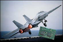 Aerospace Electronics
Military Hardware
Automotive Electronics
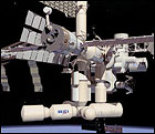
Space Exploration Equipment
Semiconductor Equipment
Outdoor Meters, Electronics, and Sensors
Oil Exploration Components
Oceanography Equipment
Medical Electronics
Telecommunication Hardware
Solvent Protection:
SCS Parylene has been tested and proven to be a successful
barrier against these organic
and inorganic solvents for electronics:
Organic Solvents
Alcohol (isopropyl)Ketones (acetone and 2, 4-pentanedione)
Aliphatic hydrocarbon (iso-octane)
Aromatic hydocarbon (xylene)
Chlorinated olefin (trichloroethylene)
Chlorinated aromatic (chlorobenzene and o-dichlorobenzene)
Heterocyclic base (pyridene)
Fluorinated solvent (trichlorotrifluroethane)
In tests, these solvents had a minor swelling effect on the Parylenes
with a 3% maximum
increase in film thickness. The swelling was found to be
completely reversible after the
solvents were removed by vacuum
drying.
 Inorganic Solvents
10% Sodium hydroxide solution
10% Ammonium hydroxide solution
10% Hydrochloric Acid solution
10% Sulfuric Acid solution
10% Nitric Acid solution
10% Chromic Acid solution
The diluted inorganic reagents had little effect on the Parylene. The
acids at 10%
concentrations had virtually no effect at room temperature
and, except for chromic, no
effect at 75°C. Concentrated acids at room
temperatures (23°C) had little effect. Under
severe conditions, 75°C for
90 minutes, all acids had a measurable effect ranging from 0.7%
swelling
with hydrochloric to 8.2% with chromic. Additionally, nitric acid under
these same
severe conditions caused severe degradation. Both concentrated
nitric and sulfuric acids
caused some discoloration.
Dielectric Protection:
SCS traditional Parylene has a dielectric constant as low as 2.65 (for
Parylene N). The
prototype Nova HT Parylene has a dielectric as low as
2.23.
Dielectric strength is important for coating circuits, lead wires, and
electronic assemblies were
bridging and arching of even trace amounts of
electrical charge can interfere with the proper
option of the
substrate.
Repair Options:
Parylene coated electronics are capable of being repaired.
To remove the Parylene for repair
options include; hard abrasion, incision
and removal, excimer laser removal, heat softening,
micro abrasion, and
plasma etching.
Removed Parylene areas can be recoated to their original tolerances by having Parylene reapplied.
Conclusion:
The unique barrier properties, the high reliability of
Parylene, and the stressless application
process makes Parylene the
preferred coating choice for hundreds of different critical electronic
applications for over three decades.
Copyright and Disclaimerc © Xuan Bao Hao Corp. 隱私保護及安全聲明 | 智慧財產權 請使用IE 4.0以上版本之瀏覽器