|   | 
            | 
           
    印刷電路板 | 
         
        
          |   | 
            | 
           
      醫療應用 | 
         
        
          |   | 
            | 
          
          磁芯上的應用 | 
         
        
          |   | 
            | 
          
          橡膠上的應用 | 
         
        
          | 
          
           | 
           
      
      微電子/微馬達 | 
         
        
          |   | 
            | 
            | 
         
        
          |   | 
            | 
          
            |  
        
          |   | 
            | 
            |  
        
          |   | 
            | 
            |  
        
          |   | 
            | 
            |  
        
          |   | 
            | 
            |  
        
          |   | 
            | 
            |  
        
          |   | 
            | 
            |  
        
          |   | 
            | 
            |  
        
          |   | 
            | 
            |  
        
          |   | 
            | 
            |  
        
          |   | 
            | 
            |  
        
          |   | 
            | 
            |  
        
          |   | 
            | 
            |  
        
          |   | 
            | 
            |  
        
          |   | 
            | 
            |  
        
          |   | 
            | 
            |  
        
          |   | 
            | 
            |  
        
          |   | 
            | 
            |    | 
      | 


              聚對二甲苯的真空氣相沉積工藝不僅和微電子積體電路製作工藝相似,而且,所製備的聚對二甲苯塗層介電常數也低,還能用微電子加工工藝進行刻蝕製圖、進行再金屬化。因此,在積體電路微電子領域中不僅可用作防護材料,而且也能作為結構層中的介電材料和製作時的掩模材料使用。經聚對二甲苯塗敷過的積體電路晶片,其25μm


              細直徑金連接線,連接強度可提高5∼10


              倍。近十年來,國外在多層積體電路和超大規摸積體電路(ULIC)


              中不斷報導在使用該材料,SCS還開發了一種耐溫更高、介電常數更低的氟代聚對二甲苯為其配套,利用真空氣相化學沉積的工藝方法,對原材料進行改性,就是在對二甲苯環二體上引入氟元素,利用該成膜方法,合成具有優異的超薄防護性能和高頻介電性能。可使防護的微波電路的頻率提高到20 
              GHz
              左右。。另外,由於聚對二甲苯低溫性能特別好,
              
                    
              I. B.M 
              
			  
              公司還用聚對二甲苯開發了一種能在液氮下工作的積體電路。 


              MEMS 
              
              作為超小型電子機械,要求使用的材料必須具有如下特性: 
                    
                    (a) 
              
              能進行微米級微細製作和加工;
              
                    
                    (b) 
              
              在微細結構中仍具有優良的電性能和物理機械性能; 
                    
                    (c) 
              
              與其他微細結構材料有很好的相容性;(d)
              
              對微電子機械系統的使用環境有很好的相容性和防護性。聚對二甲苯能在0. 
              2μm


              厚時就完全沒有針孔,5μm


              厚就能耐1 
              000 V 
              
              以上直流擊穿電壓,又是摩擦係數很低的一種自潤滑材料,化學惰性和阻隔性能也好。因此,在微電子機械系統中,聚對二甲苯除了作電介質材料外,還用作微型傳動機構和微型閥門的結構材料和防護材料。國外在這方面發展較快,經常有研究論文發表。 
               
               
              聚對二甲苯在感測器領域中的應用,除了作絕緣介質外,更多是用作防護材料。聚對二甲苯能耐酸、堿和有機溶劑,對水汽和鹽霧等惡劣環境有極好的阻隔防護能力。用極薄的聚對二甲苯作防護塗層,可以在幾乎不影響感測器功能的情況下,為傳感器提供良好的防護。這一特性引起了感測器領域的極大興趣,至今國外已有四千萬以上各種感測器用聚對二甲苯防護,其中有汽車感測器、腐蝕環境用傳感器、生物醫學用感測器、聲學感測器等等。
                    
               
              	  MEMS (Microelectromechanical System), (also called 
                    Nanotechnology) represents the highest level of 
                    micro-integration yet devised. MEMS integrate Motion, light, 
                    sound, molecular detection, radio waves, and computation. 
                    All converge on an unusual chip array, many times smaller 
                    than a grain of sand.  


                    Developments 
                    in the MEMS arena show that MEMS can be used as a DNA 
                    detector; that can sense if a DNA strand is defective. Some 
                    devices are so small that they could be injected into the 
                    human body. The day may come when micro-robots, or "Nanobots", 
                    travel through the body to clear arteries and make repairs, 
                    borrowing a scene from the classic 1960's science fiction 
                    movie Fantastic Journey. MEMS could also find 
                    military uses suggested by science fiction writers like Dean 
                    Smith who tells of battles between earth Nanobots and alien 
                    micro-machines in The Tenth Planet.  
                    
                    
                    Current MEMS Products  
                    
                    There are 
                    only a handful of MEMS products on the market but we will 
                    see a large variety come to commercial fruition during the 
                    upcoming decade. 
                    
                    
                      Accelerometers (Used with virtually all modern automotive 
                      airbags)  
                      Micro-Mirrors (MOEMS) (Used in some digital projectors) 


                    Parylene with MEMS 
                    /spacer.gif)  
                    Friction and Stiction. A common problem with the 
                    development of MEMS and MOEMS is the problem of Friction or 
                    Stiction. Friction is common to all mechanical 
                    products, however in MEMS, traditional lubricants are not 
                    practical. Stiction is a surface effect 
                    problem that is somewhat unique to micromechanical devices. 
                    The tiny MEMS elements, once they make contact with one 
                    another, are held together by surface tension and 
                    atomic-level forces (Similar to static electricity). 
                    
                    Parylene 
                    as a Friction, Stiction Solution 
                    
                    Many experts 
                    agree that a solution to the friction/stiction problem lies 
                    in an organic coating with low surface energy and, perhaps, 
                    hydrophobic properties. The coating would need to be very 
                    thin and this is the realm for vacuum coating technology. 
                    
                    
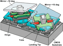
                    Given these 
                    parameters, a logical solution is Parylene. First, it is 
                    important to say that only a limited amount of study has 
                    been done in this cutting edge area of technology, but SCS 
                    is working with the industry to test several Parylenes 
                    including a newer non-stick fluorinated product. (Right: 
                    "Digital Light Processing for High-Brightness, 
                    High-Resolution Applications", Larry J. Hornbeck). 
                    
                    Parylene 
                    (poly-para-xylylene) is a high temperature polymer film 
                    applied to substrates in a vacuum chamber by means of a gas 
                    phase polymerization that provides unusual electrical and 
                    environmental performance. This class of polymer has been 
                    used for decades on a variety of applications, especially 
                    those involving the protection of electronic devices and 
                    circuitry. CVD is used to form an insulating thermoplastic 
                    coating with a high degree of chemical inertness, absence of 
                    pinholes and perfect conformity to the topography of the 
                    surface applied. Coefficients of friction range from 0.25 to 
                    0.33 so that the lubricity is close to that of Teflon. The 
                    table below summarizes the attributes of value to MEMS/MOEMS. 


                              | 
                              
                               Stress-free coatings | 
                              
                              Yes | 
                              
                              Yes | 
                             
                            
                              | 
                              
                               Thin contiguous film without pinholes | 
                              
                              Yes | 
                              
                              Yes | 
                             
                            
                              | 
                              
                               Inert | 
                              
                              Yes | 
                              
                              Yes | 
                             
                            
                              | 
                              
                               Even coating of sides and edges | 
                              
                              Yes | 
                              
                              Yes | 
                             
                            
                              | 
                              
                               Hydrophobic | 
                              
                              Yes | 
                              
                              Yes | 
                             
                            
                              | 
                              
                               Low surface energy (especially fluorinated Nova 
                              HT) | 
                              
                              Yes | 
                              
                              Yes | 
                             
                            
                              | 
                              
                               High temp. capability up to 500° C | 
                              
                              Yes | 
                              
                              Yes | 
                             
                            
                              | 
                              
                               Low k down to 2.28 | 
                              
                              Yes | 
                              
                                | 
                             
                            
                              | 
                              
                               Optically clear, UV resistant | 
                              
                                | 
                              
                              Yes | 


                      In deposition, the Parylene gas polymerizes spontaneously 
                      on the surface of coated objects that are at ambient 
                      temperature with no stresses induced initially or 
                      subsequently. There are no cure-related hydraulic or 
                      liquid surface tension forces in the process. The mean 
                      free path is only about 0.1 cm so that sides and small 
                      openings are coated. A typical rate of 0.2m or less 
                      provides precise thickness control. Polymerization occurs 
                      in crevices, under devices, and on exposed surfaces at 
                      about the same rate to give a very uniform film. Parylene 
                      coating thickness can be as low as 100 Angstroms.  
                    
                    Parylene Issues 
                     
                    There could be some issues with Parylene according to the 
                    few researchers who have experimented with the organic 
                    coatings on MEMS. Thin coatings gave good anti-stiction 
                    results before packaging but control may be difficult. Anti-stiction 
                    performance was apparently good using standard Parylene but 
                    sealing the hermetic package can cause degradation. Two 
                    recommendations were given for Parylene on MEMS devices:  
                    
                    A 
                    well-controlled deposition process for very thin coatings.
                     
                    Higher temperature stability to withstand ceramic packaging 
                    processes.


                    References  
                    
                    
                    Mignardi, M., "From ICs to DMDs", TI Technical Journal, pp. 
                    56 - 63, July - Sept. 1998 (http://www.TI.com).  
                    Miller, W. M., "MEMS Reliability and Testing", IMAPS 
                    Packaging of MEMS Microsystems Workshop, Chicago, Oct. 23 - 
                    24, 1999.
                     
                    Howe, R., et al., "Silicon Micromechanics: Sensors And 
                    Actuators On A Chip," I.E.E.E. Spectrum, Vol. 27, No. 7, pp. 
                    30-35, July 1990.  
                    Sherman, S, et al, "Monolithic Accelerometer", US Patent 
                    5,345,824, September 13, 1994. Martin, J. and Zhao, Y., "Micromachined 
                    Devices Packaged to Reduce Stiction", US Patent 5,694,740, 
                    Dec. 9, 1997. 


                 |