|
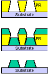
光学或电子束曝光形成光刻胶的图形,金属薄膜沉积之后将光刻胶用除胶剂等溶解清除。
剥离用负胶跟光刻原理有关。正胶是曝光部分被显影掉。光刻胶层顶部比底部的曝光量更充足,显影后形成上面小下面大的“正梯形”截面。镀金属后难剥离。负胶则相反。
NR7-PY lift-off
resist is a simple, easy method for making metallic patterns on a
substrate, especially for those noble metal thin films such as
platinum, tantalum, nickel or iron which are difficult to be
etched by conventional methods.
NR7
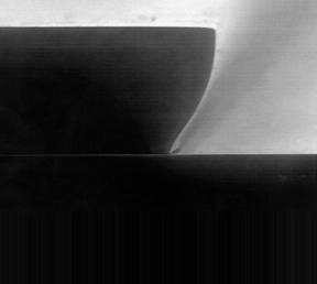
side walls with a large undercut are required for lift-off
applications. The resists make possible fabrication of side
walls with high undercut. Edge profiles with steep edges or with
high undercut can be generated by varying the development time.
Using a minimum time for development, the resist side walls can be
made steep, and only a small undercut occurs in the middle region.
With over-development,
the undercut increases - and the resulting patterns are best
suited for use with lift-off techniques. gold, aluminum, and
nickel were used for sputtering, and the metals were deposited on
the resist patterns up to a height of 1
µm. No change in resist quality was
observed during the deposition process. After metal, the resist
patterns could easily be removed with acetone.
|
High Temperature Resists |
|
Resist
NR7-1000PY
NR7-1500PY
NR7-3000PY
NR7-6000PY |
Thickness
0.7µm - 2.1µm
1.1µm - 3.1µm
2.1µm - 6.3µm
5.0µm - 12.2µm |
Temperature resistance = 180°C
for metal evaporation and sputtering |
|
|
Enhanced Adhesion |
|
Resist
NR9-1000PY
NR9-1500PY
NR9-3000PY
NR9-6000PY
NR9-8000 |
Thickness
0.7µm - 2.1µm
1.1µm - 3.1µm
2.1µm - 6.3µm
5.0µm - 12.2µm
6.0µm - 25.0µm |
|
Temperature resistance = 100°C.
for metal evaporation |
|
|
undercut |
Negative PR |
 |
|
Film
deposition |
|
PR
removal |
Advantage:
Easy to handle, fewer process steps
Temperature resistance up to
180 °C and adjustable undercut
Good line width
resolution
Deposite metal film by thermal evaporation
NR7-PY lift-off
resist can be
done using :
Acetone. Additional clean should be done using O2 plasma ash, or
photoresist developer, or Resist Remover RR4
Metallization – deposition and etching
GaN Electronics For High Power, High
Temperature Applications
Methods for fabricating Ohmic contacts to
nanowires and nanotubes
AlGaN/GaN
Heterostructure FET — Processing and Parameters Evaluation
Advanced
Manufacturing Techniques for Next Generation power FET Technology
Si-CMOS-compatible
lift-off fabrication of low-loss planar chalcogenide waveguides
If you don't find what you're looking for,
Contact Us.
We may have a suitable product that's not listed, or we may be
able to develop a material to fit your specific needs.
Tel : (02)2217-3442 / Fax : (02)2704-4070
|