|
|
|
 |
微流道微針陣列 |
|
|
化學增幅型 |
|
|
晶圓凸塊 |
| |
感光性間隙 |
| |
平坦化 |
| |
pHEMT閘極製程 |
| |
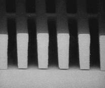
高深寬比 |
| |
厚膜光阻 |
| |
微影製程 |
| |
熱安定抗蝕刻 |
| |
側壁結構 |
| |
高深寬比電鑄模 |
| |
|
| |
|
| |
|
| |
|
| |
|
| |
|
| |
ASML PAS 5500 / 850C Stepper |
| |
Nikon stepper |
| |
TEL ACT 8 (i-line) Coater / Developer |
| |
Hitachi S-9220 CD-SEM |
| |
|
| |
|
|
| |
负性光刻胶。与曝光区域发生交联。特性:良好粘附力、良好阻挡作用、感光速度快。
有較好解析能力,
圖形縮小容易(光照速度快),
增加產能
(烘烤及顯影時間較短),
降低生產成本
乾式蝕刻
NR7 NR5系列
通過曝光能量,容易控制側壁的角度
在120°C
以下可用丙酮完全洗乾淨,
耐高溫
:
180°C
NR7經過Silylation
Process,可耐溫250°C
噴墨印刷Inkjet
printing已經成為快速成長的明星產業. 新一代微量噴墨頭Inkjet
Heads的製作上,
旋寶好化學扮演了重要的腳色
Lexmark
和HP
同時採用了NR4-8000P和NR5-8000
負型光阻開發新一代的微量噴墨頭
NR5-8000
在deep RIE , Bosch製程,可製作非常精緻的圖型
另一個NR5-8000廣泛使用
的地方是,鍍金時用NR5-8000做保護膜mask
曝光不足時,
NR5-8000
的圖型會向內凹,
因此,NR5-8000也非常適合Lift-off
製程
NR5-8000
適合大量生產用途,
有較好的解析度,線寬,厚度控制,耐高溫,PDMS接合,較短曝光和烘烤時間,任何厚度都可得到垂直的圖形,可取代正型光阻
|
 |
 |
|
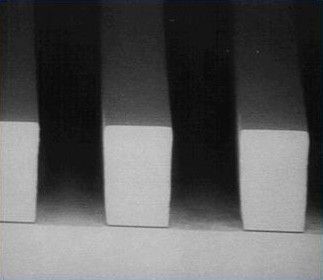
深寬比
2.1:1
|
深寬比
4.5:1
|
濕式蝕刻
NR9系列
附著力強,不需粘著增進劑
容易洗淨,可用丙酮完全洗乾淨
耐溫 度
:
100°C
NR7
NR1 系列
Under cut
可用曝光能量控制
光阻剝離 :
在120°C
以下可用丙酮完全洗乾淨
耐溫度180°C,
NR7經過 Silylation
Process
製程,可耐溫250°C
NR9 系列
附著力強,
不需粘著增進劑
容易洗淨,可用丙酮完全洗乾淨
耐溫
:
100°C
|
Negative Resists |
|
|
NR7-1000PY
0.7µm - 2.1µm
NR7-1500PY
1.1µm - 3.1µm
NR7-3000PY
2.1µm - 6.3µm
NR7-6000PY
5.0µm - 12.2µm |
|
NR9-1000PY
0.7µm - 2.1µm
NR9-1500PY
1.1µm - 3.1µm
NR9-3000PY
2.1µm - 6.3µm
NR9-6000PY
5.0µm - 12.2µm
NR9-8000
6.0µm - 25.0µm |
|
Temperature resistance
<
130°C |
|
|
型號 |
特性 |
|
NR9-PY |
用於lift-off製程,高黏附性、容易洗淨,耐高溫 |
|
NR7-PY |
用於lift-off製程,高溫,可作為永久間隔材料 |
|
NR7/NR9-PY |
用於lift-off製程,高黏附性、容易洗淨,耐高溫/做永久間隔材料 |
|
NR9-PY |
用於lift-off製程,高黏附性、容易洗淨,耐高溫 |
|
NR7-P |
做掩膜,適用於乾式蝕刻,可作永久間隔材料 |
|
NR9-P |
高黏附性,適用於電鍍和濕法蝕刻 |
|
NR5/NR7 |
可作厚膜掩膜,適用於離子蝕刻/做掩膜,可作永久間隔材料 |
|
NR2 |
可實現120um膜厚,6:1深寬比的圖案,適用於電鍍、濕法蝕刻 |
|
NR5 |
可作厚膜掩膜,適用於離子蝕刻 |
|
NR2-P |
可實現100um膜厚的凹凸圖案,解析度好,易於去除 |
|
NR9 |
增強了黏附性,適用於噴塗和輥塗 |
|
RD6 |
顯影時間短,適用於正、負性光阻劑 |
|
RR4/RR5 |
可以安全、高效的去除光阻劑及臨時塗層,適用於多種襯底材料 |
Machine Aligned
Fabrication of Submicron
Nb/Al-AlOX/Nb Junctions
using a Focused Ion Beam
A
Broadband
Surface-Micromachined
15-45 GHz Microstrip
Coupler
Enhancing reliability of
InGaN/GaN light-emitting
diodes by controlling
theetching profile of
the current blocking
layer
Integrated electroplated
heat spreaders for high
power semiconductor
lasers
InGaN/GaN
Multiple Quantum Well
Light-Emitting Diodes
grown on Polar,
Semi-polar and Non-Polar
Orientations
化學機械研磨法之垂直結構發光二極體
Layout Optimisation of
(In)GaN LEDs for
HighBrightness
Applications
Antifouling Stripes
Prepared from Clickable
Zwitterionic Copolymers
Biomedical Applications
for Microfluidic Devices
Spatial field control of
board area semiconductor
lasers with integrated
grating couplers
Simple Holographic
Patterning for
High-Aspect-Ratio
Three-Dimensional
Nanostructures with
Large Coverage Area
Full-Color Realization
of Micro-LED Displays
High efficiency membrane
light emitting diode
fabricated by back wafer
thinning technique
Heat dissipation
analysis of bendable
AlGaInP micro-LED arrays
High Breakdown Voltage
AlGaN/GaN HEMTs
Employing Recessed Gate
Edge
High-Q Tunable Silver
Capacitors for RFIC's
Design and fabrication
of GaN-based laser
diodes for single-mode
and narrow-linewidth
applications
If you don't find what you're looking for,
Contact Us.
We may have a suitable product that's not listed, or we may be
able to develop a material to fit your specific needs.
Tel : (02)2217-3442 / Fax : (02)2704-4070
|
|
|
|